| Technical Name |
The Future of 2D Materials: Transistors, Transparent Electrodes and Photodetectors |
| Project Operator |
Academia Sinica |
| Project Host |
林時彥 |
| Summary |
"Conductive 2D materials as low-contact-resistance electrodes → MoS2 transistors with all 2D material interfaces.

 van der Waals epitaxy of 2D materials → quantum-dot light-emitting diodes and bifacial solar cells with thin metal/2D material transparent electrodes.

 Resonant plasmonic nanostructures → ultrathin phototransistors with ultrahigh responsivity

Wafer-scale and multi-layer 2D materials → photovoltaic vertical devices and photoconductive planar photodetectors with shortened response times" |
| Scientific Breakthrough |
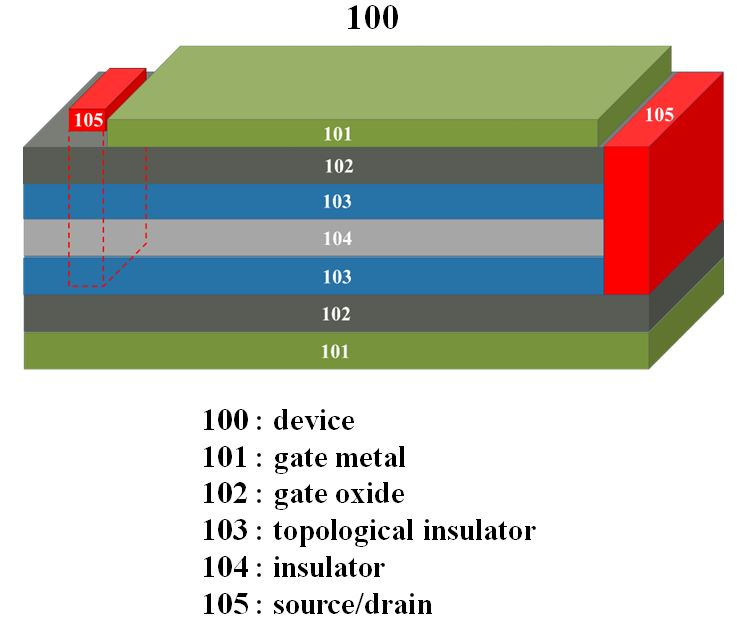
"The crystallinity of the contact electrodes and non-2D material interfaces are the main bottleneck for the performances of 2D material transistors.

 The highly conductive metal film with nanometer thicknesses grown on 2D material interfaces can be applied in backend interconnects and transparent electrodes of optical devices.

Resonant plasmonic nanostructures are applied for the fabrication of mono-layer 2D material photodetectors with high responsivities and detectivities." |
| Industrial Applicability |
"High-performance 2D material transistors → electronic devices in the < 1 nm technology node (semiconductor industry)

 Nanometer-thick metal/2D material transparent electrodes → dual-side emission quantum-dot light-emitting diodes and bifacial solar cells (display and green energy industries)

Resonant plasmonic nanostructures → photodetectors with high detectivity (LiDAR and quantum communication/computation)" |
| Keyword |
Wafer-scale 2D materials 2D material hetero-structures Transistors with all 2D material interfaces 2D material memory Low contact resistance electrodes Transparent electrodes Light-emitting diodes Solar Cells Plasmonic nanostructures Photodetectors |

