| Technical Name | Si/Ge Single-Crystal-Islands Monolithic 3D ICs Technique | ||
|---|---|---|---|
| Project Operator | National Yang Ming Chiao Tung University | ||
| Project Host | 陳冠能 | ||
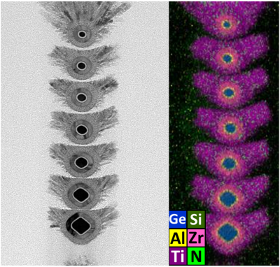
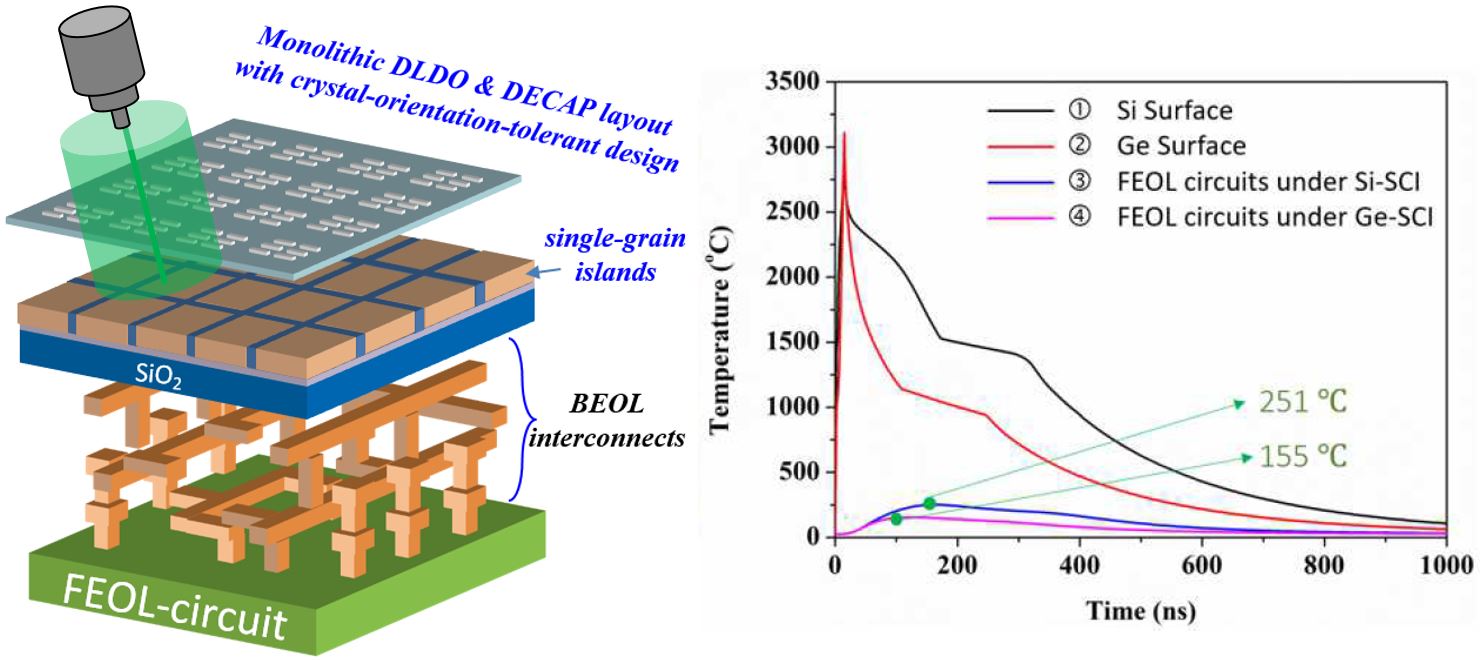
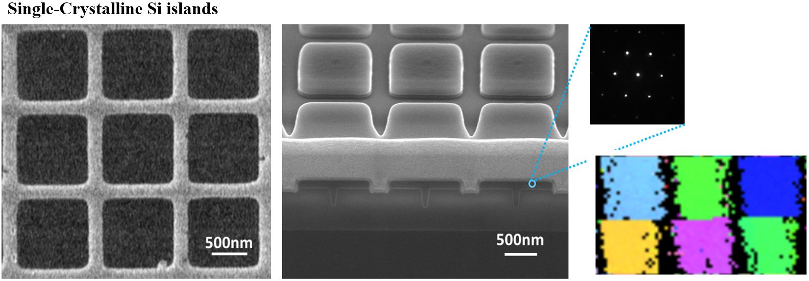
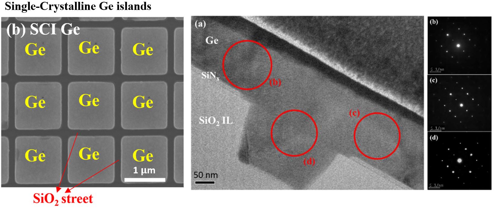
| Summary | For the single-crystal-islands (SCI) technique, structure of the cooling holesSiGe islands combining with laser crystallization was utilized to control the crystallization direction of SiGe,the single-crystalline SiGe islands with regular shape were thereby accomplished. Moreover, the SiGe FinFETs within the SCI technique would significantly improve the performanceyield of integration circuits. Therefore, this proposed technique features high-quality stackable devices, low thermal budgethigh-throughputis considered to be the key technique for the monolithic 3D ICs. |
||
| Scientific Breakthrough | For the future semiconductor architecture, monolithic 3D ICs would be one of the iconic techniques. Our team successfully utilized the single-crystal-islands (SCI) technique to fulfill the single-crystalline SiGe islands matrix with several μm2 in size. Therefore, the performanceyield of transistorscircuits would be significantly improved. The low thermal impact (300℃) of this technique on the bottom layer circuits had been also demonstrated. This single-crystal-islands technique had been demonstrated to be an important technique for future 3D ICs. |
||
| Industrial Applicability | As the IoT industry flourishing, the demands for chips with high-performance, low power consumptionmulti-function are growing. Monolithic 3D ICs featuring low cost, high-bandwidth connectivity,high heterogeneous ability has been considered critical technique for the future semiconductor. Our team’s single-crystal islands technique highly matched the industrial requests for monolithic 3D ICs: high-qualitystackable devices, low thermal budgethigh throughput, hence it would be an important technique for monolithic 3D ICs. This project is collaborating with TSMCwere published in International Electron Devices Meeting (IEDM) 2018, 2019, 2020,2021. |
||
| Keyword | Monolithic 3D ICs Single-Crystal-Islands Technique Nanosecond Laser Crystallization single-crystalline Si single-crystalline Ge Low Thermal Budget Fabrication | ||
- Contact
- Hao-Tung Chung
- don124636288@gmail.com
other people also saw


