| Technical Name | Feasible Technology for graphene application in electronic Interconnections | ||
|---|---|---|---|
| Project Operator | Chang Gung University | ||
| Project Host | 陳始明 | ||
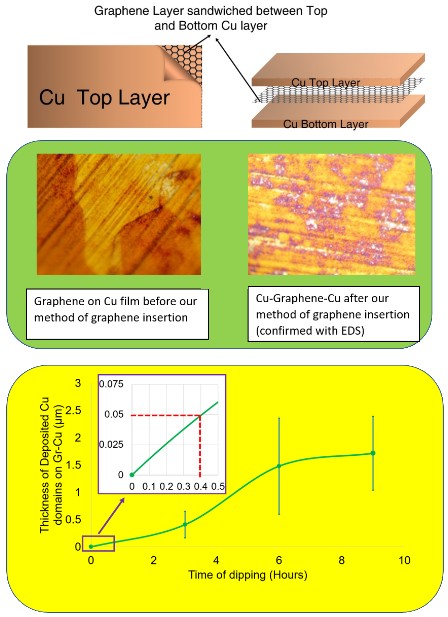
| Summary | VLSIs are facing bottlenecks due to long signal delay and short electromigration lifetime of their interconnections. Graphene (Gr) is proposed due to its excellent electrical and thermal properties, and it can be patterned by conventional microelectronic processes. |
||
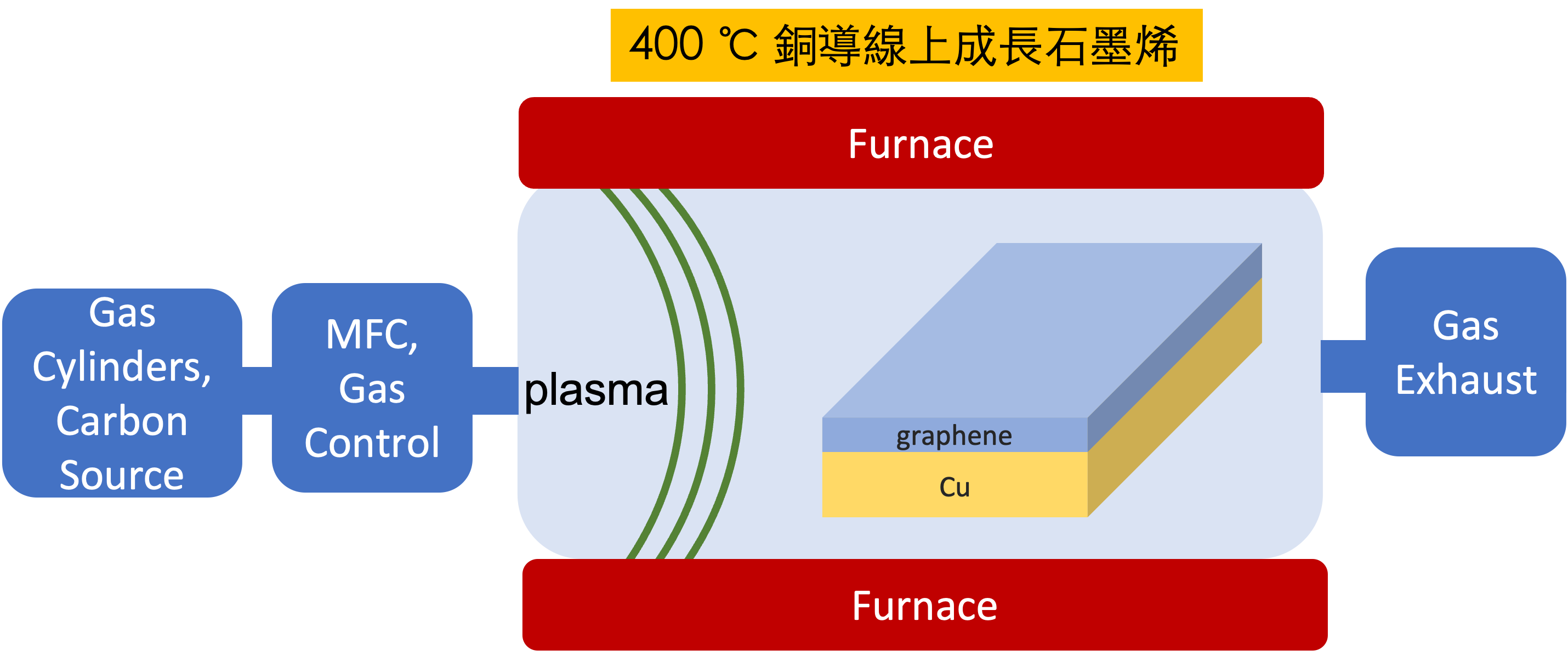
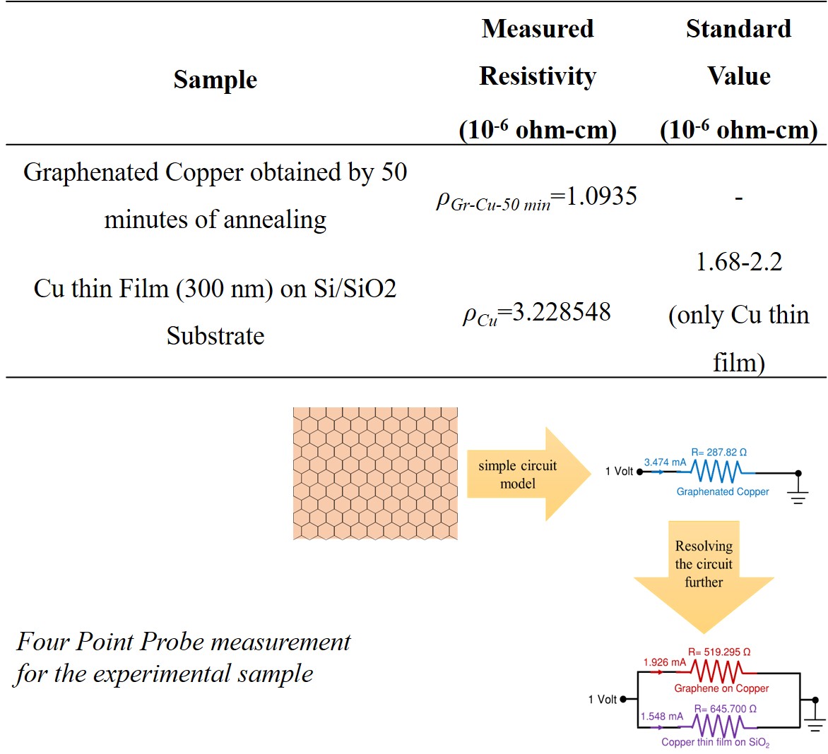
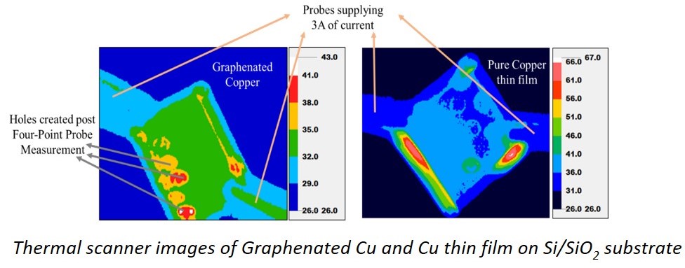
| Scientific Breakthrough | A low temperature graphene deposition on VLSI interconnections for backend process compatibility and a method of embed this graphene in VLSI interconnections so that standard mature interconnection processes can be applied. Electrical and thermal conductions will be via the embedded graphene which are excellent as compared to any metals, and electromigration reliability of such interconnect is also proven to be at least three time higher in lifetime as compare to copper. |
||
| Industrial Applicability | This technology can be used for all interconnects in both integrated circuits and printed circuit boards. The cost of this technology is low because it only requires an immersion tank of copper sulphate solution. Our technology uses a PVD process based on amorphous carbon, so graphene (Gr) deposition on interconnects can also be low temperature and cost-effective. |
||
| Keyword | Interconnections VLSI printed circuit board Copper Aluminium Wafer fabrication compatible Reliability electromigration electrochemical Graphene | ||
- crest@mail.cgu.edu.tw
other people also saw

