| Technical Name | Low temperature instant copper bondinghigh toughness/low resistance RDL lines using 111 nanotwinned copper linesfoils | ||
|---|---|---|---|
| Project Operator | National Chiao Tung University | ||
| Project Host | 陳智 | ||
| Summary | Electroplated nanotwinned Cu possesses excellent electrical & mechanical properties. It can be applied in three major joints: 1. Low thermal budget/ low resistance Cu bonding for high performance computing chip. We are able to achieve low temperature bondinginstant bonding. Low temperature bonding is performed at 150°C for 1 h to achieve low contact resistance copper bonding. Instant bonding is performed at 300°C for 5 seconds under a pressure of 90MPa achieve low contact resistance. 2. High strength/ High ductility copper lines in 3D-IC packaging We are able to fabricate high strength foils with tensile strength of 800MPa. After annealing at 150°C for 3 hours, the foil retains a tensile strength of 750MPa. 3. Cu foils for lithium ion battery |
||
| Technical Film | |||
| Scientific Breakthrough | We are able to DC electroplate highly (111) oriented nanotwinned copper filmsfabricate high strength/high conductivity/High toughness copper lines in 3D-IC packaging The tensile strength can be as high as 800MPa while maintaining reasonable ductility. After annealing at 150°C for 3 hours, the foil retains a tensile strength of 750MPa. This exhibits the ideal thermal stabilitytoughness ductility for 3D-IC application. In addition, with the Cu foils, the energy density can be increased. |
||
| Industrial Applicability | Low temp Cu-Cu bonding appears to be the solution for next generation ultra-fine pitch packaging. Nanotwinned Cu lines can also be used as redistribution lines in 3D IC integration. This technology has drawn attention from TSMC, MediaTek, Applied Materials, LAM Research,we have projects with them to co-developed some applications. In addition, this technology also drawn attention from the US |
||
| Matching Needs | 1.Cu-Cu bonding, fine pitch, low thermal budget, low resistance junction. 2.High electromigration resistancehigh strength Cu lines. 3.high strength nanotwinned Cu. |
||
| Keyword | nanotwinned copper Cu film with large grains high strength/ high thermal stability low temperature low pressure copper bondin Cu current collector for lithium ion battery Instant Cu-Cu bonding 3D IC integration AI chip packaging High electromigration resistance RDL Low resistance/ High strength Cu lines/foil | ||
| Report |
3D封裝不是夢,就靠奈米雙晶銅隨著半導體產業快速發展,晶片尺寸逐漸縮減,因此封裝技術必須隨之提升,其中晶片間之接合便是3D IC封裝技術之關鍵,現今常用的接合方式為覆晶焊錫技術,利用焊錫球與金屬反應層的冶金反應形成可靠的接點,為了提高單位面積下I/O數量,晶片尺寸需要微縮,接點間距與焊錫球直徑亦需縮小,然而,在回焊過程中發現會發生橋接失效與side wetting使得接點失效,並提出將焊錫球完全移除只剩金屬層對接利用擴散來形成可靠接點。
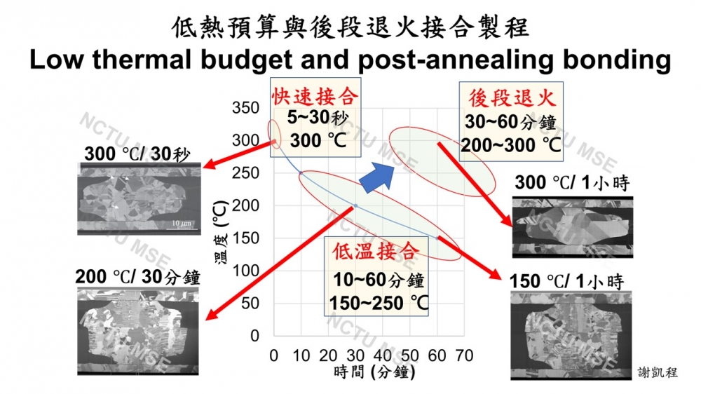
在金屬/金屬接合的低熱預算製程中,由於銅在<111>具較快之擴散速率,本研究團隊將引入具高<111>優選方向之奈米雙晶銅,主要發展出快速接合與低溫接合兩個重要方向,達到降低熱預算的要求。快速接合的溫度在300℃,而時間可壓縮至30秒內,甚至是5秒,此接合製程除了降低熱預算,還能夠加速生產速率,有望在未來完成chip-to-wafer等製程的量產;而低溫接合的溫度則可以降低到250℃以下,甚至降到150℃,在記憶體等元件封裝上有重要的價值。
在進一步探討接合時間與溫度對於接合強度之關係,在10秒和30秒內進行即時接合製程,並在300℃下進行一小時熱處理,再將試片分為未經二次退火及在氬氣氛圍下進行二次退火,探討接點強度之變化,結果顯示經二次退火之試片,其接合強度與導電性有顯著提升。
在異質接合(hybrid bonding)中主要分為聚亞醯胺(PI)/銅及非導電膠(NCP)/銅兩種接合製程,在聚亞醯胺(PI)/銅之異質接合製程中,採真空熱壓接合方式進行銅柱/PI薄膜對接PI薄膜,再升溫固化達一定固化程度,使PI同時具有可交聯性及足夠強度;透過上述製程,能夠調控PI薄膜和銅的結構,使其具有穩定的機械性質,並且仍然能夠繼續完成固化以及接合,在微電子封裝產業中具有應用潛力。在非導電膠(NCP)於奈米雙晶銅薄膜之接合製程中,能夠在大氣環境下進行接合,同時完成接合及NCP之固化,其接合強度佳,且NCP的填充性也不錯,整體具不錯之良率,未來在業界應用具有潛力,有望成為新一代之封裝技術,將奈米雙晶銅應用於接點間的接合,NCP能夠為接合提供良好保護,可望能夠成為一個不錯的解決方式。
|
||
| Download |
2012-11 Science Unidirectional growth of microbumps in nt-Cu.pdf 2015-2 Scientific Reports Cu direct bonding by nt-Cu.pdf 2020-8 Materials Tensile strength of different nt-Cu structures_down sized.pdf |
||
- chih@mail.nctu.edu.tw


