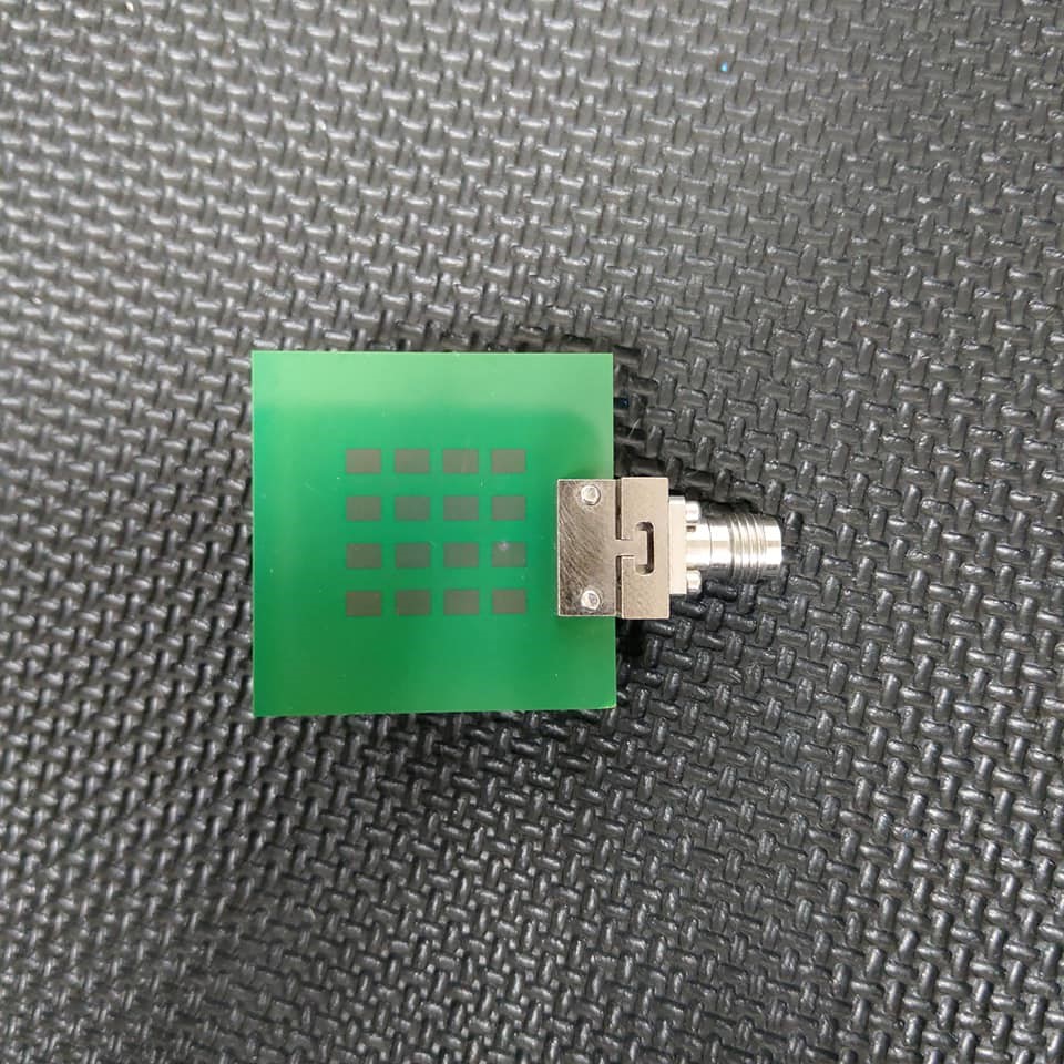
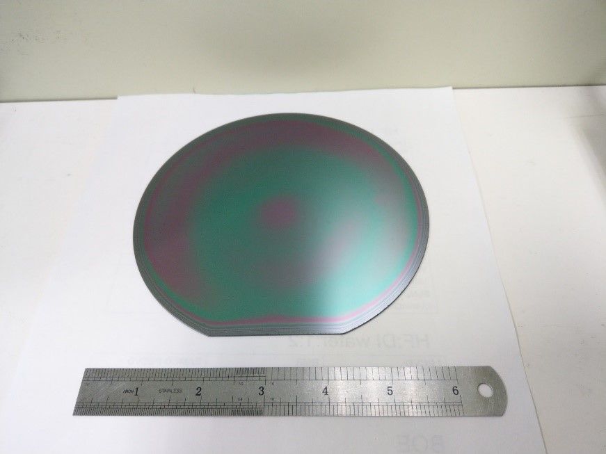
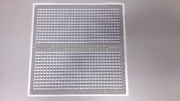
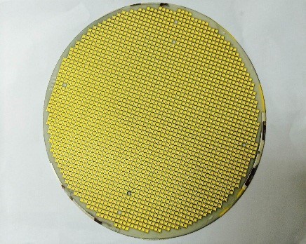
| Technical Name | Aluminum Nitride Substrate (Including Metallization Circuits) | ||
|---|---|---|---|
| Project Operator | National Chung-Shan Insitute of Science and Technology | ||
| Summary | In order to meet the requirements of 3DIC technology demands, the AlN substrate process is chosen to be developed to solve the problems of leakage current, cross talk and heat concentration in package. The adoption of AlN substrate is helpful to raise the performance and reliability of high power device with miniaturization stacking. |
||
| Scientific Breakthrough | Normally, silicon and glass is usually used as 3DIC interposer substrate material. However, Si substrate suffered the problems of leakage current and signal noise due to its worse electrical insulation, and Glass substrate suffered the severe problems of heat dissipating due to its worse thermal conductivity. In order to solve the above mentioned problems, we develop the AlN substrate material with high electrical insulation and thermal conductivity to meet the demands of 3DIC interposer substrate application. |
||
| Industrial Applicability | 散熱基板、陶瓷構裝基板、3DIC中介層基板 |
||
other people also saw

